Page 107 - System on Package_ Miniaturization of the Entire System
P. 107

Stacked ICs and Packages (SIP)      83


                        Si chip carrier  stacking  A.D Scarbrough  Basic TSV technology  MPU chip  50μm 20μm  SDRAM chip
                                 Stack
                                 interconnection
                                 wafers
                                 Memory chip
                                 wafer
                                                                                Au bump
                                 combined
                                 interconnection
                                 & spacer wafer
                            Memory
                                                                                  30μm interposer chip
                                 Selection and
                            Element
                            Portion
                                 driving circuitry
                                 wafer
                                                                                  30μm
                                                                                Under fill
                              (1971)
                                                                                   Two layer
                                                                               200μm
                                                                                   substrate
                     TSV                GE (1981)   Bosch (1994)      IME (2003)  Solder bump
                         Chip stacking   RPI, GE & IBM  True-silicon  ASET (2001)  Samsung (2006)
                                           (1986)
                 SIP technologies  Package stacking  IBM (1973)  GM (1983)  CSF (1993)  carriers  Intel & tessera(2001)  (2006)
                                                         (1999)
                                                                          IBM
                                                                                        Intel
                                                                          (2005)
                                                       Thomson-
                                DIP
                                  Piggyback
                                  Socket
                                 DIP
                                                              Chip
                                  PCB
                                                       Metal
                                                       traces
                     Non-TSV   Standard socket   DIP  White microelectronics (1994)  Pad Conductive  Top die  Bumps  Under fill
                                                                       Sharp (2001)
                                                              Epoxy
                               Bell Lab (1969)
                                                       ICs
                                                         Wire bond
                                                   Substrate
                         Chip stacking                Matra marconi  Bottom die  Memory device 5  IMEC & fujitsu (2001)
                                                                                 AMKOR (2001)
                                                      space(1993)
                                                                          Memory device 4
                                                                          Memory device 3
                                                                          Memory device 2
                                             Irvine (1992)
                          1970    1980    1990                    2000    Memory device 1  2010
                                                      Year
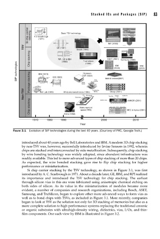
               FIGURE 3.1  Evolution of SIP technologies during the last 40 years. (Courtesy of PRC, Georgia Tech.)
                    introduced about 40 years ago by Bell Laboratories and IBM. A modern 3D chip stacking
                    by non-TSV was, however, successfully introduced by Irvine Sensors in 1992, wherein
                    chips are stacked and interconnected by side metallization. Subsequently, chip stacking
                    by wire bonding technology was widely adopted, since abundant infrastructure was
                    readily available. This led to more advanced types of chip stacking of more than 20 chips.
                    As expected, the wire bonded stacking gave rise to flip chip stacking for higher
                    performance or miniaturization.
                       Si chip carrier stacking by the TSV technology, as shown in Figure 3.1, was first
                    introduced by A. C. Scarbrough in 1971. About a decade later, GE, IBM, and RPI realized
                    its importance and introduced the TSV technology for chip stacking. The earliest
                    through-silicon vias in this era were fabricated using anisotropic chemical etching on
                    both sides of silicon.  As its value in the miniaturization of modules became more
                    evident, a number of companies and research organizations, including Bosch, ASET,
                    Samsung, and TruSilicon, began to explore other more advanced ways to form vias as
                    well as to bond chips with TSVs, as included in Figure 3.1. More recently, companies
                    began to look at TSV as the solution not only for 3D stacking of memories but also as a
                    more complete solution to high-performance systems replacing the traditional ceramic
                    or organic substrates with ultrahigh-density wiring, dielectrics, vias, I/Os, and thin-
                    film components. One such view by IBM is illustrated in Figure 3.2.
   102   103   104   105   106   107   108   109   110   111   112