
Page 110 - System on Package_ Miniaturization of the Entire System
P. 110
Stacked ICs and Packages (SIP) 85
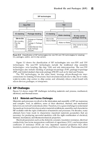
SIP technologies
Non-TSV TSV
IC stacking Package stacking IC stacking
Wafer stacking Si chip carrier
package stacking
Die-to-Die - Die-to-Die
- Package-on-Package
- Wire bonding (PoP) - Die-to-Wafer
- Flip chip - Package-in-Package - Wafer-to-Wafer
- TAB (PiP) - Chip carrier-to-chip
- Side - Folded-Stacked Chip carrier
interconnection Scale Package
(FSCSP)
FIGURE 3.3 Classifi cation of SIP technologies into non-TSV and TSV technologies for stacking
ICs, packages, wafers, and Si chip carriers.
Figure 3.3 shows the classification of SIP technologies into non-TSV and TSV
technologies. The non-TSV technologies include the traditional chip assembly
technologies—wire bonding, flip chip, TAB, and side interconnection. The non-TSV
technologies also include stacking of package-on-package (PoP), package-in-package
(PiP), and folded-stacked chip-scale package (FSCSP) such as by Intel and Tessera.
The TSV technologies, on the other hand, leverage silicon-through-via inter-
connections for forming 3D structures. Such structures include die-to-die, die-to-wafer,
wafer-to-wafer, chip carrier–to–chip carrier, and ultimately silicon circuit board with
silicon devices, packages, or interposers.
3.2 SIP Challenges
Figure 3.4 shows major SIP challenges including materials and process, mechanical,
electrical, and thermal issues.
3.2.1 Materials and Process Challenges
Materials and processes involved in the fabrication and assembly of SIP are numerous
and complex. And, in addition, some of their electrical, thermal, and mechanical
behaviors are not well understood either. Therefore, it is a great challenge to understand
the needs up front and develop or select materials to fabricate, assemble, and characterize
SIP modules with the right combination of materials and processes. For decades, many
attempts have been made to characterize important materials parameters that are
necessary for producing successful modules with the right combination of electrical,
thermal, mechanical, and thermomechanical properties.
Electrical parameters such as the dielectric constant, insulation resistance, electrical
conductivity, loss factor, temperature coefficient of capacitance (TCC), and temperature
coefficient of resistance (TCR) are very important material properties that affect
insulators, resistors, capacitors, inductors, and filters, to name a few. Thermomechanical