
Page 114 - System on Package_ Miniaturization of the Entire System
P. 114
Stacked ICs and Packages (SIP) 89
each interconnection such as a wire bond, transmission line, via, or solder ball needs to
increase. From a signal integrity point of view, a higher interconnect speed means a more
difficult package design due to the constraints of package size, layer number, and cost. For
example, with the data rate under 50 MHz, a chip-scale package can be treated as a circuit
block with R (resistor), L (inductor), and C (capacitor) elements and the impact on signal
integrity is limited. However, when frequency goes to 500 MHz or greater, a package is no
longer a “small” portion of the signal propagation path, and “full wave” theory behavior
must be considered. As a result, the package design and associated technology need to pay
specific attention to electrical performance. First, the signal path on the package level needs
a well-designed reference and return path. For example, each signal line needs its nearby
power or ground path for reference as well as for crosstalk shielding. An excellent reference
design means more power or ground connections per signal and that can prove costly.
Therefore, accurate predictions for the right ratio of signal to power not only provide good
performance, but also the lowest cost. Second, the package design needs to provide a path
for higher IC power delivery. For cost and form factor reasons, it would not be desirable to
put decoupling capacitors on the package. Parasitic inductance, therefore, from the package
needs to be extremely slow in order to minimize voltage fluctuations during circuit switching.
The way to keep a clean power supply for stacked die packages is to mainly focus on package
V (source voltage) and V (collector voltage) design for the lowest loop inductance. Although
ss
cc
on-die decoupling capacitors help to reduce power noise, it is usually not the first choice due
to the added cost factor. Third, electrical package design requires consideration of
electromagnetic inference (EMI) and electromagnetic compatibility (EMC). With higher-
density wire bonds in place, coupling between wire bonds becomes more significant. The
problem becomes more severe when high-power circuits are close to lower-power circuits.
For example, when RF circuits and digital circuits are within one package, the electrical
design needs to make special considerations for the isolation between digital and RF in order
to minimize the EMI and EMC impacts.
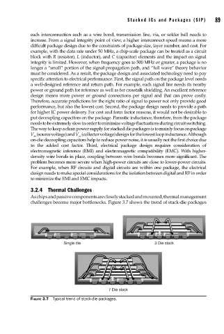
3.2.4 Thermal Challenges
As chips and passive components are closely stacked and mounted, thermal management
challenges become major bottlenecks. Figure 3.7 shows the trend of stack-die packages
Single die 3 Die stack
7 Die stack
FIGURE 3.7 Typical trend of stack-die packages.