
Page 118 - System on Package_ Miniaturization of the Entire System
P. 118
Stacked ICs and Packages (SIP) 93
Finally, it is very important to validate the optimized SIP design from thermal simulation
by using either thermal test vehicles or the actual products. This is the only way to
ensure that the product meets all the specifications.
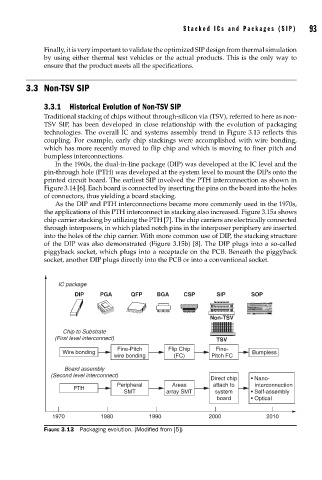
3.3 Non-TSV SIP
3.3.1 Historical Evolution of Non-TSV SIP
Traditional stacking of chips without through-silicon via (TSV), referred to here as non-
TSV SIP, has been developed in close relationship with the evolution of packaging
technologies. The overall IC and systems assembly trend in Figure 3.13 reflects this
coupling. For example, early chip stackings were accomplished with wire bonding,
which has more recently moved to flip chip and which is moving to finer pitch and
bumpless interconnections.
In the 1960s, the dual-in-line package (DIP) was developed at the IC level and the
pin-through hole (PTH) was developed at the system level to mount the DIPs onto the
printed circuit board. The earliest SIP involved the PTH interconnection as shown in
Figure 3.14 [6]. Each board is connected by inserting the pins on the board into the holes
of connectors, thus yielding a board stacking.
As the DIP and PTH interconnections became more commonly used in the 1970s,
the applications of this PTH interconnect in stacking also increased. Figure 3.15a shows
chip carrier stacking by utilizing the PTH [7]. The chip carriers are electrically connected
through interposers, in which plated notch pins in the interposer periphery are inserted
into the holes of the chip carrier. With more common use of DIP, the stacking structure
of the DIP was also demonstrated (Figure 3.15b) [8]. The DIP plugs into a so-called
piggyback socket, which plugs into a receptacle on the PCB. Beneath the piggyback
socket, another DIP plugs directly into the PCB or into a conventional socket.
IC package
DIP PGA QFP BGA CSP SIP SOP
Non-TSV
Chip to Substrate
(First level interconnect) TSV
Fine-Pitch Flip Chip Fine-
Wire bonding Bumpless
wire bonding (FC) Pitch FC
Board assembly
(Second level interconnect)
Direct chip • Nano-
Peripheral Areas attach to interconnection
PTH
SMT array SMT system • Self-assembly
board • Optical
1970 1980 1990 2000 2010
FIGURE 3.13 Packaging evolution. (Modifi ed from [5])