
Page 120 - System on Package_ Miniaturization of the Entire System
P. 120
Stacked ICs and Packages (SIP) 95
In response to the need for higher-density printed wiring boards (PWBs), the 1980s saw
the development of surface-mount technology (SMT) and the quad-flat package (QFP).
Since packages such as QFP used in SMT have leads and not pins, they can be mounted
on both surfaces of the PWB, leading to higher-density packaging. The QFP allows a
lead frame to run around on all four sides of a square package, thus enabling higher pin
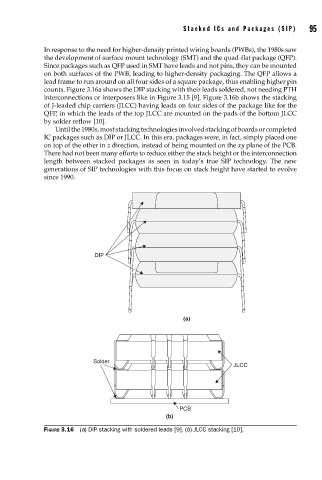
counts. Figure 3.16a shows the DIP stacking with their leads soldered, not needing PTH
interconnections or interposers like in Figure 3.15 [9]. Figure 3.16b shows the stacking
of J-leaded chip carriers (JLCC) having leads on four sides of the package like for the
QFP, in which the leads of the top JLCC are mounted on the pads of the bottom JLCC
by solder reflow [10].
Until the 1980s, most stacking technologies involved stacking of boards or completed
IC packages such as DIP or JLCC. In this era, packages were, in fact, simply placed one
on top of the other in z direction, instead of being mounted on the xy plane of the PCB.
There had not been many efforts to reduce either the stack height or the interconnection
length between stacked packages as seen in today’s true SIP technology. The new
generations of SIP technologies with this focus on stack height have started to evolve
since 1990.
DIP
(a)
Solder
JLCC
PCB
(b)
FIGURE 3.16 (a) DIP stacking with soldered leads [9]. (b) JLCC stacking [10].