
Page 125 - System on Package_ Miniaturization of the Entire System
P. 125
100 Cha pte r T h ree
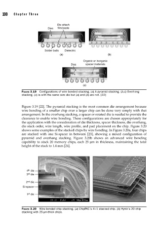
Die attach
Dies film/paste
Solder balls Dielectric
(a) (b)
Organic or inorganic
Dies spacer materials
(c)
FIGURE 3.19 Confi gurations of wire bonded stacking. (a) A pyramid stacking. (b,c) Overhang
stacking. (c) is with the same size die but (a) and (b) are not. [22]
Figure 3.19 [22]. The pyramid stacking is the most common die arrangement because
wire bonding of a smaller chip over a larger chip can be done very simply with that
arrangement. In the overhang stacking, a spacer or rotated die is needed to provide the
clearance to enable wire bonding. These configurations are chosen appropriately for
the application with the consideration of die thickness, spacer thickness, die overhang,
die stack order, wire length, wire profile, and pad placement on the chip. Figure 3.20
shows some examples of the stacked chips by wire bonding. In Figure 3.20a, four chips
are stacked with one Si-spacer in between [23], showing a mixed configuration of
pyramid and overhang stacking. Figure 3.20b shows an advanced wire bonding
capability to stack 20 memory chips, each 25 μm in thickness, maintaining the total
height of the stack to 1.4 mm [24].
4 th die
3 rd die
2 nd die
Si-spacer
1 die
st
FIGURE 3.20 Wire bonded chip stacking. (a) ChipPAC’s 4+1 stacked chip. (b) Hynix’s 20 chip
stacking with 25-μm-thick chips.