
Page 130 - System on Package_ Miniaturization of the Entire System
P. 130
Stacked ICs and Packages (SIP) 105
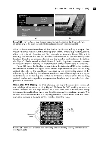
Top grinding
185μ proven
Self aligning
solder
Underfilling process
proven gam
<28μ
SnAg
Wire-bondable Solderable
Pd UBM Pd UBM
Bottom
grinding
(a) (b)
FIGURE 3.25 (a) Two face-to-face chips connected by microbumps in a fl ip chip architecture.
(b) Bottom chip of the stack connected to the substrate through wire bonding. [30]
this short interconnection enables miniaturization by eliminating long wire spans that
would otherwise be needed to bond the top chip. For this type of chip stacking, bottom
chips need both wire bonding and flip chip pads, as shown in Figure 3.26. In this
stacking, the bottom dies are first attached and connected to the substrate by wire
bonding. Then, the top dies are attached face down on the front surface of the bottom
die. Figure 3.25b shows such stacked chips with the flip chip interconnections between
two dies and the wire bonding for interconnection of the bottom dies to the substrate.
Figure 3.27 shows the flip chip bonded bottom die in the stack [32]. In this stacking,
the bottom die operates at a higher speed with its high number of I/Os. This stacking
method also relieves the bond-finger crowding in one concentrated region of the
substrate by redistributing the substrate density to two different regions: the region
under the die for the flip chip and further out for the wire bonded chips. This stacking
method has been developed for next-generation handsets and is extendable to other
products in the future.
Chip-on-Chip (COC) Stacking In COC stacking, flip chip interconnections connect all
stacked chips without wire bonding. Figure 3.28 shows the COC stacking structure, in
which subchips are flip chip bonded on a base chip with ultrafine-pitch bump
interconnection and the base chip is also flip chip mounted on a package substrate. This
method allows the connection of a very large number of I/Os in the stack and thus a
significant increase in the data transfer speed between the chips.
FIGURE 3.26 Bond pads of bottom dies for fl ip chip and wire bonding stacking with the bottom
dies fl ipped. [31]