
Page 131 - System on Package_ Miniaturization of the Entire System
P. 131
106 Cha pte r T h ree
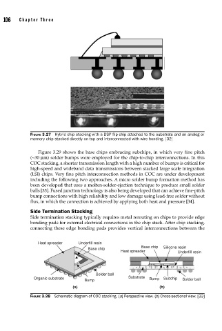
FIGURE 3.27 Hybrid chip stacking with a DSP fl ip chip attached to the substrate and an analog or
memory chip stacked directly on top and interconnected with wire bonding. [32]
Figure 3.29 shows the base chips embracing subchips, in which very fine pitch
(~30 μm) solder bumps were employed for the chip-to-chip interconnections. In this
COC stacking, a shorter transmission length with a high number of bumps is critical for
high-speed and wideband data transmissions between stacked large scale integration
(LSI) chips. Very fine pitch interconnection methods in COC are under development
including the following two approaches. A micro solder bump formation method has
been developed that uses a molten-solder-ejection technique to produce small solder
balls [33]. Fused junction technology is also being developed that can achieve fine-pitch
bump connections with high reliability and low damage using lead-free solder without
flux, in which the connection is achieved by applying both heat and pressure [34].
Side Termination Stacking
Side termination stacking typically requires metal rerouting on chips to provide edge
bonding pads for external electrical connections in the chip stack. After chip stacking,
connecting these edge bonding pads provides vertical interconnections between the
Heat spreader Underfill resin
Base chip Silicone resin
Base chip
Heat spreader Underfill resin
Solder ball
Organic substrate Substrate Bump Subchip Solder ball
Bump
(a) (b)
FIGURE 3.28 Schematic diagram of COC stacking. (a) Perspective view. (b) Cross-sectional view. [33]