
Page 136 - System on Package_ Miniaturization of the Entire System
P. 136
Stacked ICs and Packages (SIP) 111
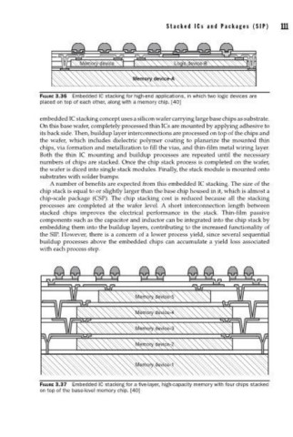
Memory device Logic device-B
Memory device-A
FIGURE 3.36 Embedded IC stacking for high-end applications, in which two logic devices are
placed on top of each other, along with a memory chip. [40]
embedded IC stacking concept uses a silicon wafer carrying large base chips as substrate.
On this base wafer, completely processed thin ICs are mounted by applying adhesive to
its back side. Then, buildup layer interconnections are processed on top of the chips and
the wafer, which includes dielectric polymer coating to planarize the mounted thin
chips, via formation and metallization to fill the vias, and thin-film metal wiring layer.
Both the thin IC mounting and buildup processes are repeated until the necessary
numbers of chips are stacked. Once the chip stack process is completed on the wafer,
the wafer is diced into single stack modules. Finally, the stack module is mounted onto
substrates with solder bumps.
A number of benefits are expected from this embedded IC stacking. The size of the
chip stack is equal to or slightly larger than the base chip housed in it, which is almost a
chip-scale package (CSP). The chip stacking cost is reduced because all the stacking
processes are completed at the wafer level. A short interconnection length between
stacked chips improves the electrical performance in the stack. Thin-film passive
components such as the capacitor and inductor can be integrated into the chip stack by
embedding them into the buildup layers, contributing to the increased functionality of
the SIP. However, there is a concern of a lower process yield, since several sequential
buildup processes above the embedded chips can accumulate a yield loss associated
with each process step.
Memory device-5
Memory device-4
Memory device-3
Memory device-2
Memory device-1
FIGURE 3.37 Embedded IC stacking for a fi ve-layer, high-capacity memory with four chips stacked
on top of the base-level memory chip. [40]