
Page 141 - System on Package_ Miniaturization of the Entire System
P. 141
116 Cha pte r T h ree
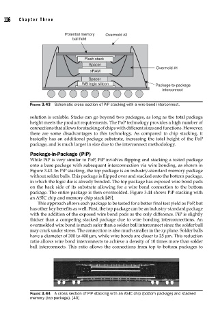
Potential memory Overmold #2
ball field
Flash stack
Spacer
Overmold #1
xRAM
Spacer
WB logic silicon Package-to-package
interconnect
FIGURE 3.43 Schematic cross section of PiP stacking with a wire bond interconnect.
solution is scalable. Stacks can go beyond two packages, as long as the total package
height meets the product requirements. The PoP technology provides a high number of
connections that allows for stacking of chips with different sizes and functions. However,
there are some disadvantages to this technology. As compared to chip stacking, it
basically has an additional package substrate, increasing the total height of the PoP
package, and is much larger in size due to the interconnect methodology.
Package-in-Package (PiP)
While PiP is very similar to PoP, PiP involves flipping and stacking a tested package
onto a base package with subsequent interconnection via wire bonding, as shown in
Figure 3.43. In PiP stacking, the top package is an industry-standard memory package
without solder balls. This package is flipped over and stacked onto the bottom package,
in which the logic die is already bonded. The top package has exposed wire bond pads
on the back side of its substrate allowing for a wire bond connection to the bottom
package. The entire package is then overmolded. Figure 3.44 shows PiP stacking with
an ASIC chip and memory chip stack [49].
This approach allows each package to be tested for a better final test yield as PoP, but
has other key benefits as well. First, the top package can be an industry-standard package
with the addition of the exposed wire bond pads as the only difference. PiP is slightly
thicker than a competing stacked package due to wire bonding interconnections. An
overmolded wire bond is much safer than a solder ball interconnect since the solder ball
may crack under stress. The connection is also much smaller in the xy plane. Solder balls
have a diameter of 300 to 400 μm, while wire bonds are closer to 25 μm. This reduction
ratio allows wire bond interconnects to achieve a density of 10 times more than solder
ball interconnects. This ratio allows the connections from top to bottom packages to
FIGURE 3.44 A cross section of PiP stacking with an ASIC chip (bottom package) and stacked
memory (top package). [49]