
Page 137 - System on Package_ Miniaturization of the Entire System
P. 137
112 Cha pte r T h ree
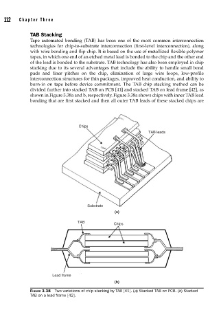
TAB Stacking
Tape automated bonding (TAB) has been one of the most common interconnection
technologies for chip-to-substrate interconnection (first-level interconnection), along
with wire bonding and flip chip. It is based on the use of metallized flexible polymer
tapes, in which one end of an etched metal lead is bonded to the chip and the other end
of the lead is bonded to the substrate. TAB technology has also been employed in chip
stacking due to its several advantages that include the ability to handle small bond
pads and finer pitches on the chip, elimination of large wire loops, low-profile
interconnection structures for thin packages, improved heat conduction, and ability to
burn-in on tape before device commitment. The TAB chip stacking method can be
divided further into stacked TAB on PCB [41] and stacked TAB on lead frame [42], as
shown in Figure 3.38a and b, respectively. Figure 3.38a shows chips with inner TAB lead
bonding that are first stacked and then all outer TAB leads of these stacked chips are
Chips
TAB leads
Substrate
(a)
TAB
Chips
Lead frame
(b)
FIGURE 3.38 Two variations of chip stacking by TAB [41]. (a) Stacked TAB on PCB. (b) Stacked
TAB on a lead frame [42].