
Page 142 - System on Package_ Miniaturization of the Entire System
P. 142
Stacked ICs and Packages (SIP) 117
increase dramatically over other stacked solutions. In addition, this methodology is also
not sensitive to bus technology. One-, two-, or four-sided buses can be connected.
However, wires are much thinner and have much higher resistance and much lower
current carrying capability than solder balls. Long wires can severely affect high-
frequency performance. In addition, since this package uses wire bonds as the primary
interconnect, most customers will have to buy this unit as a complete system. It is also
doubtful that an industry-standard interface could be obtained given the complex
nature of how the interconnect is formed.
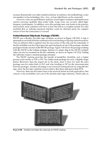
Folded-Stacked Chip-Scale Package (FSCSP)
FSCSP uses a flexible, thin-film tape substrate, as shown in Figure 3.45 [50]. A chip is
mounted on one-half of the flex substrate with wire bonding or flip chip interconnections.
Then an adhesive film is applied onto the top surface of the chip and the remainder of
the flex is folded over the chip to provide open land pads on top of the package. Another
package is finally stacked on the FSCSP package. Figure 3.46 shows the package stacking
with the FSCSP as the bottom package. Instead of a single chip in the FSCSP, multiple
chips can also be mounted on the flex substrate, as shown in Figure 3.47 [51]. Folding
the substrate creates a stacked package structure.
The FSCSP stacking provides the benefit of testability, flexibility, and a higher
process yield similar to PoP or PiP. The folded stack package has only a slightly larger
planar dimension than the largest die in the stack, since it does not need the extra
package area for solder balls in PoP and wire bonding in PiP for the interconnection
between packages. Another advantage is an increased routing density by using the flex
tape, since the flex tape substrate process allows finer lines and spaces than PCB.
However, there are still some issues to be resolved before its wide application. One
concern is the availability and cost of the double-sided tape substrate, which adds an
FIGURE 3.45 Unfolded and folded fl ex substrate for FSCSP stacking.