
Page 146 - System on Package_ Miniaturization of the Entire System
P. 146
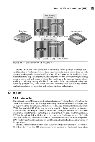
Stacked ICs and Packages (SIP)      121


                                                   ASIC/memory
                                                      combo


                                                         Package stack


                          Chip stack        Chip stack                       Package stack

                                          2 Chip  3 Chip  4 Chip 5 Chip or more
                                                  Memory combo

                                                         Package stack

                                            Chip stack


                                          2 Chip  3 Chip  4 Chip 5 Chip or more
                    FIGURE 3.49  Selection of non-TSV SIP solutions. [53]


                       Figure 3.49 shows some guidelines to select chip versus package stackings. For a
                    small number of IC stacking (two or three chips), chip stacking is competitive for both
                    memory stacking and combined stacking of logic IC and memory. For stacking a higher
                    number of chips, chip stacking may still be competitive with a low cost for high-yielding
                    memory chips, but with expensive logic ICs combined with memory chips, package
                    stacking is definitely more preferable. In conclusion, balancing and optimizing cost,
                    flexibility, performance, form factor, and time-to-market will result in the optimal
                    application solution between chip and package stacking technologies.


               3.4 TSV SIP

                    3.4.1 Introduction
                    The main drivers for 3D interconnections in packaging are (1) size reduction, (2) solving the
                    “interconnect bottleneck,” (3) heterogeneous integration of different technologies, and
                    (4) higher electrical performance. International Technology Roadmap for Semiconductors
                    (ITRS) has identified 3D IC stacking as a way to achieve better electrical performance
                    without further shrinking of transistor dimensions. Through-silicon via (TSV) has been
                    identified as one of the major technologies to achieve the above goals by 3D integration. A
                    TSV is a through-via hole drilled in silicon (die, wafer, or Si chip carrier) and filled with
                    conductor material to form vertical electrical interconnections in modules or subsystems.
                    TSVs run through the silicon die and are used to connect vertically stacked dies, wafers, or
                    Si chip carriers.
                       Figure 3.50 shows the historical trend in system integration leading to TSV-enabled
                    3D integration. The first 2D interconnect is an example of horizontal integration