
Page 151 - System on Package_ Miniaturization of the Entire System
P. 151
126 Cha pte r T h ree
There have been quite a few products introduced in the market with 3D TSV
technology. Tru-Si Technologies began marketing its Thru-Silicon vias in late 1999 [64].
The Association of Super-Advanced Electronics Technologies (ASET) developed a 3D
die-stacked module in which four ultrathin chips (50 μm thick) are vertically stacked
and have electrically interconnected Cu-filled through-hole vias [65]. IME developed a
3D silicon chip carrier stacking technology (using TSVs) in 2003 [66]. In 2005, Hitachi
and Renesas developed another 3D stacking technology with TSVs with gold stud
bumps [67]. In this approach, a compressive force is applied at room temperature to
electrically connect the gold stud bumps on upper chips to through-hole-via electrodes
in the lower chips. In April 2006, Samsung Electronics announced that it had developed
a wafer-level processed stack package (WSP) of high-density memory chips using TSV-
based 3D interconnection technology [68]. Samsung’s WSP is a 16-Gbit memory solution
that stacked eight 2-Gb NAND chips. In September 2006, Intel developed a prototype
processor with 80 cores [69]. It used 3D TSV technology to stack 256 kbytes of SRAM
directly on top of each of the chip’s 80 cores. In June 2007, IBM announced SiGe BiCMOS
5PAe technology, which uses through-silicon vias for 3D stacking [70].
In addition to the above, there are several others who are also actively working in
the area of 3D TSV integration technology. Some of them are Micron, Tezzaron,
Ziptronics, Lincoln Labs, and RTI in the United States; NEC, Oki, Elpidia, Toshiba, and
Zycube in Japan; and IMEC, Fraunhofer IZM, and LETI in Europe.
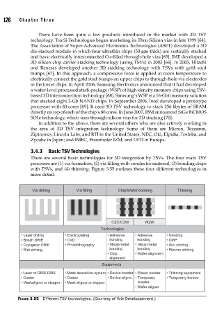
3.4.3 Basic TSV Technologies
There are several basic technologies for 3D integration by TSVs. The four main TSV
processes are (1) via formation, (2) via filling with conductor material, (3) bonding chips
with TSVs, and (4) thinning. Figure 3.55 outlines these four different technologies in
more detail.
Thinning
Via drilling Via filling Chip/Wafer bonding Thinning
C2C/C2W W2W
W2W
Technologies
• Laser drilling • Electroplating • Adhesive • Adhesive • Grinding
• Bosch DRIE • CVD bonding bonding • CMP
• Cryogenic DRIE • Photolithography • Metal-metal • Metal-metal • Wet etching
• Wet etching bonding bonding • Plasma etching
• Chip • Wafer alignment
alignment
Equipments
• Laser or DRIE DRIE • Mask deposition system • Device bonder • Waver bonder • Thinning equipment
• Coater • Coater • Device aligne • Temporary • Temporary bonder
• Maskaligner or stepper • Mask aligner or stepper bonder
• Wafer aligner
FIGURE 3.55 Different TSV technologies. (Courtesy of Yole Developpement.)