
Page 152 - System on Package_ Miniaturization of the Entire System
P. 152
Stacked ICs and Packages (SIP) 127
Via Drilling
The TSVs can be formed by Bosch-type deep reactive ion etching (DRIE) [60], cryogenic
DRIE, laser drilling, or by a variety of wet etching (isotropic and anisotropic) processes.
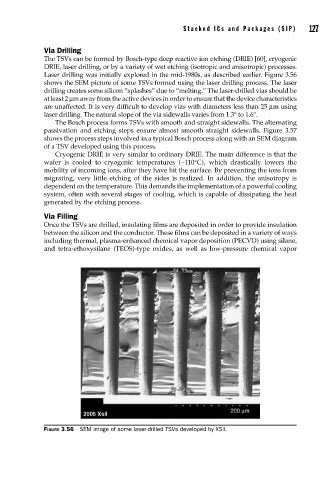
Laser drilling was initially explored in the mid-1980s, as described earlier. Figure 3.56
shows the SEM picture of some TSVs formed using the laser drilling process. The laser
drilling creates some silicon “splashes” due to “melting.” The laser-drilled vias should be
at least 2 μm away from the active devices in order to ensure that the device characteristics
are unaffected. It is very difficult to develop vias with diameters less than 25 μm using
laser drilling. The natural slope of the via sidewalls varies from 1.3° to 1.6°.
The Bosch process forms TSVs with smooth and straight sidewalls. The alternating
passivation and etching steps ensure almost smooth straight sidewalls. Figure 3.57
shows the process steps involved in a typical Bosch process along with an SEM diagram
of a TSV developed using this process.
Cryogenic DRIE is very similar to ordinary DRIE. The main difference is that the
wafer is cooled to cryogenic temperatures (−110°C), which drastically lowers the
mobility of incoming ions, after they have hit the surface. By preventing the ions from
migrating, very little etching of the sides is realized. In addition, the anisotropy is
dependent on the temperature. This demands the implementation of a powerful cooling
system, often with several stages of cooling, which is capable of dissipating the heat
generated by the etching process.
Via Filling
Once the TSVs are drilled, insulating films are deposited in order to provide insulation
between the silicon and the conductor. These films can be deposited in a variety of ways
including thermal, plasma-enhanced chemical vapor deposition (PECVD) using silane,
and tetra-ethoxysilane (TEOS)-type oxides, as well as low-pressure chemical vapor
FIGURE 3.56 SEM image of some laser-drilled TSVs developed by XSil.