Page 157 - System on Package_ Miniaturization of the Entire System
P. 157

132    Cha pte r  T h ree


                                               Glass

                       Glass

                       SOI
                               Box
                                               Si                      Si
                               (a)                      (b)                     (c)

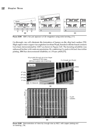
                    FIGURE 3.64  IBM’s Via Last approach of 3D integration using oxide bonding. [77]

                    Cu-through vias will eliminate the formation of bumps on the chip back surface [78].
                    High-aspect-ratio copper vias at pitches less than 50 μm, bonded with tin-based contacts
                    have been demonstrated by ASET as shown in Figure 3.65. The bonding reliability was
                    enhanced further with resin encapsulation. By combining Cu pads with lead-free solder
                    plating, IBM has demonstrated reliability at a 50-μm pitch [74].


                                   20-μm pitch through-via in the 4 layer
                                        stacking of TEG chips
                                    (SEM photograph after Si etching)  Cu-through-via (10 μm)
                                    Top chip
                                                                                 Oxide

                                                                                 Resin
                            4 th  chip
                            3 rd  chip
                            2 nd  chip
                            1 st  chip
                                     Si interposer
                                                        (a)


                                μm             20 μm pitch
                                ~50
                                                                            Cu 3 Sn
                                                                            eutecitic
                                  gap < 10 μm       Cu through via (TV)


                                   Micro thin       Interconnection of Cu TV 3


                                               COMPO    X450  10 μm
                                                     (b)
                    FIGURE 3.65  Demonstration of interchip through vias by ASET, with copper plating and
                    Sn bonding. [78]
   152   153   154   155   156   157   158   159   160   161   162