
Page 154 - System on Package_ Miniaturization of the Entire System
P. 154
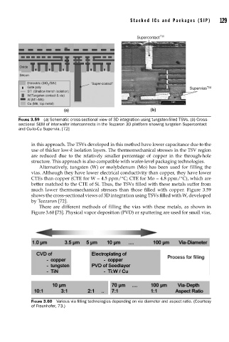
Stacked ICs and Packages (SIP)      129


                                                               Supercontact TM


               Oxide
               Silicon
                   Dielectric (SiO 2 /SiN)  “Super-contact”
                   Gate poly                                                        Supervias TM
                   STI (Shallow trench isolation)
                   W(Tungsten contact & via)
                   Al (M1–M5)
                   Cu (M6, top metal)
                                 (a)                                (b)
               FIGURE 3.59  (a) Schematic cross-sectional view of 3D integration using tungsten-fi lled TSVs. (b) Cross-
               sectional SEM of interwafer interconnects in the Tezzaron 3D platform showing tungsten Supercontact
               and Cu-to-Cu Supervia. [72]


                    in this approach. The TSVs developed in this method have lower capacitance due to the
                    use of thicker low-k isolation layers. The thermomechanical stresses in the TSV region
                    are reduced due to the relatively smaller percentage of copper in the through-hole
                    structure. This approach is also compatible with wafer-level packaging technologies.
                       Alternatively, tungsten (W) or molybdenum (Mo) has been used for filling the
                    vias. Although they have lower electrical conductivity than copper, they have lower
                    CTEs than copper (CTE for W = 4.5 ppm/°C; CTE for Mo = 4.8 ppm/°C), which are
                    better matched to the CTE of Si. Thus, the TSVs filled with these metals suffer from
                    much lower thermomechanical stresses than those filled with copper. Figure 3.59
                    shows the cross-sectional views of 3D integration using TSVs filled with W, developed
                    by Tezzaron [72].
                       There are different methods of filling the vias with these metals, as shown in
                    Figure 3.60 [73]. Physical vapor deposition (PVD) or sputtering are used for small vias,


                    FIGURE 3.60  Various via fi lling technologies depending on via diameter and aspect ratio. (Courtesy
                    of Fraunhofer, 73.)