
Page 158 - System on Package_ Miniaturization of the Entire System
P. 158
Stacked ICs and Packages (SIP) 133
Direct Cu-Cu Bonding Direct Cu-Cu bonding eliminates the tin or gold bumping
steps as well as several electrical and mechanical reliability issues associated with
solders and intermetallics. This approach makes 3D technologies more compatible
with standard wafer fabrication processes. Earlier fundamental studies on thermo-
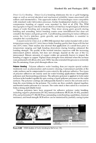
compression bonding of copper were reported by Reif et al. [79]. The TEM
micrographs in Figure 3.66 show the evolution of interface morphologies at different
stages of wafer bonding and annealing. They show strong grain growth during
bonding and annealing. Initial bonding causes some interdiffusion but does not
complete the fusion and grain growth. A postbonding annealing to induce diffusion
across the Cu-Cu interface, grain growth, and recrystallization is essential to
complete the crystallization.
A recent work by Chen et al. at IBM [80] reported that wafers bonded with a slow
temperature ramp rate (6°C/min) have a better bonding quality than those with the fast
rate (32°C/min). Their studies also showed that application of a small force prior to
temperature ramping and high bonding down-force during bonding enhanced the
bonding strength. The quality of the bonded interface improves with the increasing
interconnect pattern density, but does not strongly depend on the size of the Cu
interconnect. Minute amounts of copper oxides are generally known to impact the
bonding of copper to copper. Highest shear strengths were obtained when the surfaces
were pretreated with dilute citric acid. IMEC has also extended this process to extremely
thin Si containing 10-μm pitch through-silicon vias.
Polymer Bonding Polymer adhesive wafer bonding does not require special surface
treatments such as planarization and excessive cleaning. Contaminant particles at the
wafer surfaces can be compensated to some extent by the polymer adhesive. Two types
of polymer adhesives are mainly used for wafer bonding applications: thermoplastic
polymers and thermosetting polymers. The adhesive polymer is applied to both wafer
surfaces to be bonded together by spin coating a liquid polymer precursor on the wafer
surfaces. The polymer coatings are subsequently heated to remove the solvents and to
form the cross-linking in the polymer. The wafers are then carefully aligned together,
and bonded under pressure in a vacuum. The wafer stack is then cured in a vacuum to
form a strong and reliable bond.
Various polymers have been proposed for adhesive polymer wafer bonding,
including negative photoresists [81–82], benzocyclobutene (BCB) [64, 83–85], parylene
[76], and polyimides [77, 86]. BCB has outstanding wafer bonding capabilities, chemical
resistance, and bond strength. BCB reflow can be minimized by partially curing it prior
Si (220)
Cu
C Cu
Ta
0.5 μm Ta
Si 0.5 μm
Si
FIGURE 3.66 XTEM studies of Cu-Cu bonding by Reif et al. [79].