
Page 163 - System on Package_ Miniaturization of the Entire System
P. 163
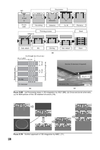
Via process
                          SiO


                            Al pad
                             Si                      Dielectric     Cu
                            Device
                                        Via etching  Dielectric    Cu fill    Planarize
                            wafer
                                            Thinning process                     Stack
                                 Adhesive
                          Substrate


                           Sub. attach    BG         Etching     Sub. detach    Stack
                                                       (a)
                               Cu-through via (10 μm sq.)
                        20 μm pitch
                                               μm
                                               50                   Stacked Si devices (4-layered)
                      Encapsulate resin        μm  10  Connecting Cu-through via   50 μm × 4


                         Si chip
                         Si interposer                        Interposer (Si)
                                                                                      1 mm
                                  (b)                                       (c)
                    FIGURE 3.69  (a) Processing steps in 3D integration by ASET [88]. (b) Cross-sectional schematic.
                    (c) An SEM picture of the 3D stacked structure [78].


                    FIGURE 3.70  Via-fi rst approach of 3D integration by IMEC. [71]

               138