
Page 167 - System on Package_ Miniaturization of the Entire System
P. 167
142 Cha pte r T h ree
LDD or TIA IC
Optochip OE
Optocard SLC Waveguide
(a)
DRIE etch of vias followed by
dielectric and liner deposition
Cu sidewall plating followed by
composite paste fill
Fabrication of BEOL wiring and
etching of through cavity
IC
Wafer thinning, backside metallurgy,
and IC-OE assembly
(b)
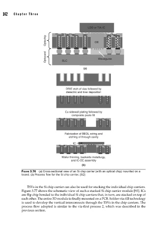
FIGURE 3.76 (a) Cross-sectional view of an Si chip carrier (with an optical chip) mounted on a
board. (b) Process fl ow for the Si chip carrier. [92]
TSVs in the Si chip carrier can also be used for stacking the individual chip carriers.
Figure 3.77 shows the schematic view of such a stacked Si chip carrier module [93]. ICs
are flip chip bonded to the individual Si chip carriers that, in turn, are stacked on top of
each other. The entire 3D module is finally mounted on a PCB. Solder-via-fill technology
is used to develop the vertical interconnects through the TSVs in the chip carriers. The
process flow adopted is similar to the via-first process 2, which was described in the
previous section.