
Page 168 - System on Package_ Miniaturization of the Entire System
P. 168
Stacked ICs and Packages (SIP) 143
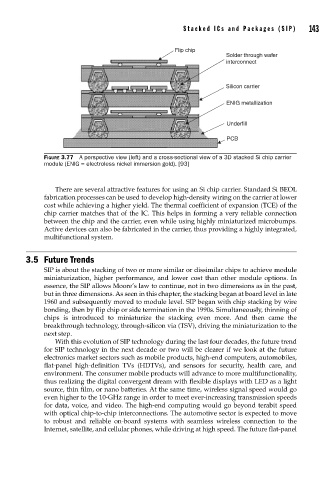
Flip chip
Solder through wafer
interconnect
Silicon carrier
ENIG metallization
Underfill
PCB
FIGURE 3.77 A perspective view (left) and a cross-sectional view of a 3D stacked Si chip carrier
module (ENIG = electroless nickel immersion gold). [93]
There are several attractive features for using an Si chip carrier. Standard Si BEOL
fabrication processes can be used to develop high-density wiring on the carrier at lower
cost while achieving a higher yield. The thermal coefficient of expansion (TCE) of the
chip carrier matches that of the IC. This helps in forming a very reliable connection
between the chip and the carrier, even while using highly miniaturized microbumps.
Active devices can also be fabricated in the carrier, thus providing a highly integrated,
multifunctional system.
3.5 Future Trends
SIP is about the stacking of two or more similar or dissimilar chips to achieve module
miniaturization, higher performance, and lower cost than other module options. In
essence, the SIP allows Moore’s law to continue, not in two dimensions as in the past,
but in three dimensions. As seen in this chapter, the stacking began at board level in late
1960 and subsequently moved to module level. SIP began with chip stacking by wire
bonding, then by flip chip or side termination in the 1990s. Simultaneously, thinning of
chips is introduced to miniaturize the stacking even more. And then came the
breakthrough technology, through-silicon via (TSV), driving the miniaturization to the
next step.
With this evolution of SIP technology during the last four decades, the future trend
for SIP technology in the next decade or two will be clearer if we look at the future
electronics market sectors such as mobile products, high-end computers, automobiles,
flat-panel high-definition TVs (HDTVs), and sensors for security, health care, and
environment. The consumer mobile products will advance to more multifunctionality,
thus realizing the digital convergent dream with flexible displays with LED as a light
source, thin film, or nano batteries. At the same time, wireless signal speed would go
even higher to the 10-GHz range in order to meet ever-increasing transmission speeds
for data, voice, and video. The high-end computing would go beyond terabit speed
with optical chip-to-chip interconnections. The automotive sector is expected to move
to robust and reliable on-board systems with seamless wireless connection to the
Internet, satellite, and cellular phones, while driving at high speed. The future flat-panel