Page 164 - System on Package_ Miniaturization of the Entire System
P. 164

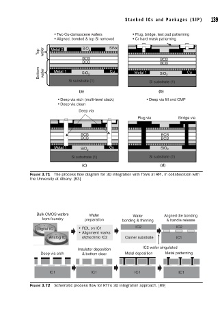
Stacked ICs and Packages (SIP)      139


                              • Two Cu-damascene wafers        • Plug, bridge, test pad patterning
                              • Aligned, bonded & top Si removed  • Cr hard mask patterning

                        Top   wafer  Metal 2  SiO 2   SiNx
                                          BCB                              BCB
                                          BCB                              BCB
                        Bottom  wafer  Metal 1  SiO 2  Cu       Metal 1    SiO 2      Cu

                                    Si substrate (1)                  Si substrate (1)

                                         (a)                              (b)
                                • Deep via etch (multi-level stack)   • Deep via fill and CMP
                                • Deep via clean
                                         Deep via
                                                                 Plug via          Bridge via


                                          BCB                              BCB
                                          BCB                              BCB

                              Metal 1    SiO 2        Cu                   SiO 2
                                      Si substrate (1)                Si substrate (1)
                                          (c)                              (d)

                    FIGURE 3.71  The process fl ow diagram for 3D integration with TSVs at RPI, in collaboration with
                    the University at Albany. [83]


                       Bulk CMOS wafers      Wafer             Wafer         Aligned die bonding
                         from foundry      preparation     bonding & thinning  & handle release

                       Digital IC        •  RDL on IC1          IC2               IC2
                                         • Alignment marks
                            Analog IC      etched into IC2  Carrier substrate     IC1

                                                                    IC2 wafer singulated
                                        Insulator deposition
                         Deep via etch    & bottom clear    Metal deposition  Metal patterning


                            IC1               IC1               IC1                IC1


                    FIGURE 3.72  Schematic process fl ow for RTI’s 3D integration approach. [89]
   159   160   161   162   163   164   165   166   167   168   169