
Page 159 - System on Package_ Miniaturization of the Entire System
P. 159
134 Cha pte r T h ree
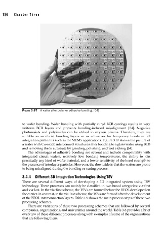
FIGURE 3.67 A wafer after polymer adhesive bonding. [64]
to wafer bonding. Wafer bonding with partially cured BCB coatings results in very
uniform BCB layers and prevents bonding-induced misalignment [84]. Negative
photoresists and polyimides can be etched in oxygen plasma. Therefore, they are
suitable as sacrificial bonding layers or as adhesives for temporary bonds in 3D
integration platforms such as for MEMS applications. Figure 3.67 shows the picture of
a wafer with Cu-oxide interconnect structures after bonding to a glass wafer using BCB
and removing the Si substrate by grinding, polishing, and wet etching [64].
The advantages of adhesive bonding are several and include compatibility with
integrated circuit wafers, relatively low bonding temperatures, the ability to join
practically any kind of wafer material, and a lower sensitivity of the bond strength to
the presence of interlayer particles. However, the downside is that the wafers are prone
to being misaligned during the bonding or curing process.
3.4.4 Different 3D Integration Technologies Using TSV
There are several different ways of developing a 3D integrated system using TSV
technology. These processes can mainly be classified in two broad categories: via-first
and via-last. In the via-first scheme, the TSVs are formed before the BEOL developed on
the carrier. In contrast, in the via-last scheme, the TSVs are formed after the development
of the BEOL interconnection layers. Table 3.5 shows the main process steps of these two
processing schemes.
There are variations of these two processing schemes that are followed by several
companies, organizations, and universities around the world. Table 3.6 provides a brief
overview of these different processes along with examples of some of the organizations
that are following them.