
Page 160 - System on Package_ Miniaturization of the Entire System
P. 160
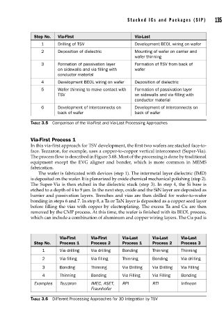
Stacked ICs and Packages (SIP)      135


                      Step No.  Via-First                      Via-Last
                         1     Drilling of TSV                 Development BEOL wiring on wafer
                         2     Deposition of dielectric        Mounting of wafer on carrier and
                                                               wafer thinning
                         3     Formation of passivation layer   Formation of TSV from back of
                               on sidewalls and via filling with   wafer
                               conductor material
                         4     Development BEOL wiring on wafer  Deposition of dielectric
                         5     Wafer thinning to make contact with   Formation of passivation layer
                               TSV                             on sidewalls and via filling with
                                                               conductor material
                         6     Development of interconnects on   Development of interconnects on
                               back of wafer                   back of wafer

                    TABLE 3.5  Comparison of the Via-First and Via-Last Processing Approaches


                    Via-First Process 1
                    In this via-first approach for TSV development, the first two wafers are stacked face-to-
                    face. Tezzaron, for example, uses a copper-to-copper vertical interconnect (Super-Via).
                    The process flow is described in Figure 3.68. Most of the processing is done by traditional
                    equipment except the EVG aligner and bonder, which is more common in MEMS
                    fabrication.
                       The wafer is fabricated with devices (step 1). The intermetal layer dielectric (IMD)
                    is deposited on the wafer. It is planarized by oxide chemical mechanical polishing (step 2).
                    The Super-Via is then etched in the dielectric stack (step 3). In step 4, the Si base is
                    etched to a depth of 4 to 9 μm. In the next step, oxide and the SiN layer are deposited as
                    barrier and passivation layers. Trenches and vias are then drilled for wafer-to-wafer
                    bonding in steps 6 and 7. In step 8, a Ta or TaN layer is deposited as a copper seed layer
                    before filling the vias with copper by electroplating. The excess Ta and Cu are then
                    removed by the CMP process. At this time, the wafer is finished with its BEOL process,
                    which can include a combination of aluminum and copper wiring layers. The Cu pad is


                                Via-First    Via-First    Via-Last    Via-Last    Via-Last
                      Step No.  Process 1    Process 2    Process 1   Process 2   Process 3
                         1      Via drilling  Via drilling  Bonding   Thinning    Thinning

                         2      Via filling  Via filling  Thinning    Bonding     Via drilling
                         3      Bonding      Thinning     Via Drilling  Via Drilling  Via Filling
                         4      Thinning     Bonding      Via Filling  Via Filling  Bonding
                      Examples  Tezzaron     IMEC, ASET,   RPI        RTI         Infineon
                                             Fraunhofer

                    TABLE 3.6  Different Processing Approaches for 3D Integration by TSV