
Page 156 - System on Package_ Miniaturization of the Entire System
P. 156
Stacked ICs and Packages (SIP) 131
Cu Adhesive
SiO 2 SiO 2 Inter-level dielectric
(a) (b) (c)
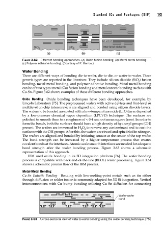
FIGURE 3.62 Different bonding approaches. (a) Oxide fusion bonding. (b) Metal-metal bonding.
(c) Polymer adhesive bonding. (Courtesy of P. Garrou.)
Wafer Bonding
There are different ways of bonding die-to-wafer, die-to-die, or wafer-to-wafer. Three
generic types are reported in the literature. They include silicon dioxide (SiO ) fusion
2
bonding, metal-metal bonding, and polymer adhesive bonding. Metal-metal bonding
can be of two types: metal (Cu) fusion bonding and metal eutectic bonding such as with
Cu-Sn. Figure 3.62 shows examples of these different bonding approaches.
Oxide Bonding Oxide bonding techniques have been developed, for example, by
Lincoln Laboratory [75]. The preprocessed wafers with active devices and first-level or
multilevel on-chip interconnects are aligned and bonded using silicon dioxide layers.
The wafers to be bonded are coated with a low-temperature oxide (LTO) layer deposited
by a low-pressure chemical vapor deposition (LPCVD) technique. The surfaces are
polished to smooth them to a roughness of < 0.4 nm root mean square (rms). In order to
form the bonds, both the surfaces should have a high density of hydroxyl groups (OH)
present. The wafers are immersed in H O to remove any contaminant and to coat the
2
2
surfaces with the OH groups. After this, the wafers are rinsed and spin dried in nitrogen.
The wafers are aligned and bonded by initiating contact at the center of the top wafer.
The bond strength can be increased by a higher-temperature process that creates
covalent bonds at the interfaces. Atomic-scale smooth interfaces are needed for adequate
bond strength after the wafer bonding process. Figure 3.63 shows a schematic
representation of this approach.
IBM used oxide bonding in its 3D integration platform [76]. The wafer bonding
process is compatible with back-end-of-the-line (BEOL) wafer processing. Figure 3.64
shows a schematic process flow of the IBM process.
Metal-Metal Bonding
Cu-Sn Eutectic Bonding Bonding with low-melting-point metals such as tin either
through diffusion or solder fusion is commonly adapted for 3D Si integration. Vertical
interconnections with Cu bump bonding utilizing Cu-Sn diffusion for connecting
Wafer-wafer
bond
FIGURE 3.63 A cross-sectional view of wafer-to-wafer bonding using the oxide bonding technique. [75]