
Page 153 - System on Package_ Miniaturization of the Entire System
P. 153
128 Cha pte r T h ree
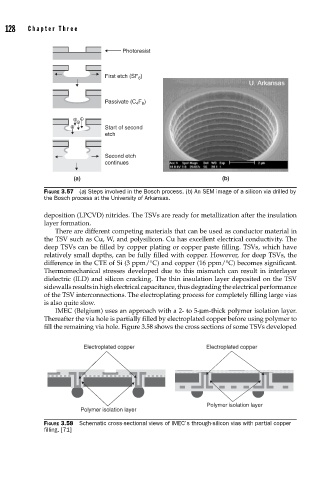
Photoresist
First etch (SF )
6
F )
Passivate (C 4 8
+ +
+
+ + Start of second
etch
Second etch
continues
(a) (b)
FIGURE 3.57 (a) Steps involved in the Bosch process. (b) An SEM image of a silicon via drilled by
the Bosch process at the University of Arkansas.
deposition (LPCVD) nitrides. The TSVs are ready for metallization after the insulation
layer formation.
There are different competing materials that can be used as conductor material in
the TSV such as Cu, W, and polysilicon. Cu has excellent electrical conductivity. The
deep TSVs can be filled by copper plating or copper paste filling. TSVs, which have
relatively small depths, can be fully filled with copper. However, for deep TSVs, the
difference in the CTE of Si (3 ppm/°C) and copper (16 ppm/°C) becomes significant.
Thermomechanical stresses developed due to this mismatch can result in interlayer
dielectric (ILD) and silicon cracking. The thin insulation layer deposited on the TSV
sidewalls results in high electrical capacitance, thus degrading the electrical performance
of the TSV interconnections. The electroplating process for completely filling large vias
is also quite slow.
IMEC (Belgium) uses an approach with a 2- to 5-μm-thick polymer isolation layer.
Thereafter the via hole is partially filled by electroplated copper before using polymer to
fill the remaining via hole. Figure 3.58 shows the cross sections of some TSVs developed
Electroplated copper Electroplated copper
Polymer isolation layer
Polymer isolation layer
FIGURE 3.58 Schematic cross-sectional views of IMEC’s through-silicon vias with partial copper
fi lling. [71]