
Page 149 - System on Package_ Miniaturization of the Entire System
P. 149
124 Cha pte r T h ree
Die-to-Die Stacking Wafer-to-Wafer Stacking
1. Different sized dies can be stacked. 1. Individual die sizes must match.
2. Alignment is easier. 2. Alignment is more difficult.
3. It uses known good die (KGD) for stacking; 3. There is a lower yield because of
hence, there is a much higher yield. KGD issues.
4. Throughput is lower. 4. Throughput is higher.
TABLE 3.4 Die-to-Die Stacking versus Wafer-to-Wafer Stacking
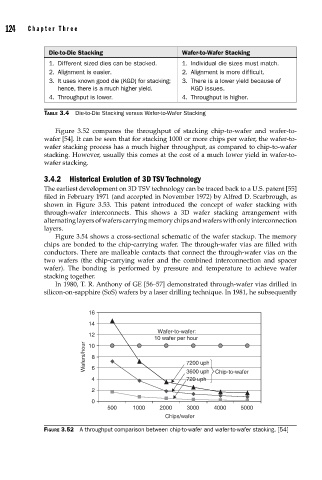
Figure 3.52 compares the throughput of stacking chip-to-wafer and wafer-to-
wafer [54]. It can be seen that for stacking 1000 or more chips per wafer, the wafer-to-
wafer stacking process has a much higher throughput, as compared to chip-to-wafer
stacking. However, usually this comes at the cost of a much lower yield in wafer-to-
wafer stacking.
3.4.2 Historical Evolution of 3D TSV Technology
The earliest development on 3D TSV technology can be traced back to a U.S. patent [55]
filed in February 1971 (and accepted in November 1972) by Alfred D. Scarbrough, as
shown in Figure 3.53. This patent introduced the concept of wafer stacking with
through-wafer interconnects. This shows a 3D wafer stacking arrangement with
alternating layers of wafers carrying memory chips and wafers with only interconnection
layers.
Figure 3.54 shows a cross-sectional schematic of the wafer stackup. The memory
chips are bonded to the chip-carrying wafer. The through-wafer vias are filled with
conductors. There are malleable contacts that connect the through-wafer vias on the
two wafers (the chip-carrying wafer and the combined interconnection and spacer
wafer). The bonding is performed by pressure and temperature to achieve wafer
stacking together.
In 1980, T. R. Anthony of GE [56–57] demonstrated through-wafer vias drilled in
silicon-on-sapphire (SoS) wafers by a laser drilling technique. In 1981, he subsequently
16
14
Wafer-to-wafer:
12
10 wafer per hour
Wafers/hour 8 7200 uph
10
6
720 uph
4 3600 uph Chip-to-wafer
2
0
500 1000 2000 3000 4000 5000
Chips/wafer
FIGURE 3.52 A throughput comparison between chip-to-wafer and wafer-to-wafer stacking. [54]