
Page 147 - System on Package_ Miniaturization of the Entire System
P. 147
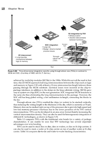
122    Cha pte r  T h ree


                  Integration technologies                             3D integration by TSV

                                                                       • Miniaturization
                                                                       • Shorter interconnects
                                                                        between functions

                                                  SOC integration
                                                                   layer
                                               • Large die
                                               • Design, time-to-market  Transistor  3D via
                                                process issues
                                                                                       M3
                                                                                       M2
                                                                                       M1
                         2D interconnect                                              Normal
                      • Long interchip                   Through-                      vias
                        connections between              silicon-via
                        logic & memory                   (TSV)      d
                                                                          3D via pade
                                                       Year

               FIGURE 3.50  Three-dimensional integration benefi ts using through-silicon vias (TSVs) in contrast to
               MCM and SOC. (Courtesy of IMEC and Dr. P. Garrou.)


                    achieved by multichip modules (MCMs) in the 1980s. While this served the need at that
                    time, this 2D MCM approach had long interconnections between the chips such as logic
                    and memory in Figure 3.50 with at least a 10-mm interconnection length between these
                    passing through the MCM substrate. Electrical losses were incurred at the chip-to-
                    package interfaces, in addition to the delays in the long substrate wiring. MCMs gave
                    way to system-on-chip (SOC) in the next generation. SOC integrated MCM functions in
                    the same die thus eliminating the long interconnections in the package. However, the
                    SOC still has long global wiring, a few millimeters in length, connecting the blocks in
                    the die.
                       Through-silicon vias (TSVs) enabled the chips (or wafers) to be stacked vertically,
                    thus reducing the wiring length to the thickness of the die, which is currently at 70 μm.
                    Memory dies can be stacked right on top of the processor die to provide high-speed and
                    low-loss memory-processor interfaces due to the lower parasitics of the TSV vertical
                    interconnections. TSVs can be developed in an area array format thereby increasing the
                    vertical interconnection density. They can also be used for heterogeneous integration of
                    different IC technologies, as shown in Figure 3.51.
                       Table 3.3 compares TSVs with the traditional wire bonds for a variety of package
                    characteristics. It can readily be seen that TSV technology has several important
                    advantages over wire bonding.
                       TSVs can be used to stack dies on dies, dies on wafers, or dies on Si chip carriers. It
                    can also be used to stack a wafer or Si chip carrier on top of another wafer or Si chip
                    carrier. Table 3.4 compares die-to-die and wafer-to-wafer stacking characteristics.