
Page 143 - System on Package_ Miniaturization of the Entire System
P. 143
118 Cha pte r T h ree
Overmold
Adhesive
Flex substrate
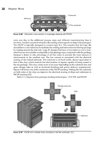
FIGURE 3.46 Schematic cross section of a package stacking with FSCSP.
extra cost due to the additional process steps and different manufacturing lines it
involves. Another concern is related to the routing of bus signals on chips to be packaged.
The FSCSP is typically designed to contain logic ICs. This requires that the logic die
should have a one-sided bus to facilitate the routing and interconnect to the top package
by routing around the fold side. Logic IC designs that have a two-sided or even a four-
sided bus are not suitable or adaptable to this package type, consistent with the package
designer’s desire to take advantage of all four sides to provide the most amount of
interconnects in the smallest area. The last concern is associated with the electrical
routing of the folded substrate. The substrate is of fixed width, almost equivalent to
that of the chip, which restricts the total number of signals capable of being routed to
the top package. This may create more of an issue depending on the substrate line and
space design rules as well as electrical shielding and power delivery requirements.
Figure 3.48 shows one of the variations of the FSCSP stacking. Folding the flex substrate
on both sides of the chip can improve the electrical routing of chips and substrates in
FSCSP stacking [52].
Table 3.1 compares three package stacking technologies—PoP, PiP, and FSCSP.
Flexible substrate
Chip
Adhesive
FIGURE 3.47 FSCSP with multiple chips mounted on the fl ex substrate. [51]