
Page 145 - System on Package_ Miniaturization of the Entire System
P. 145
120 Cha pte r T h ree
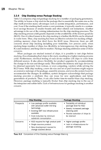
3.3.4 Chip Stacking versus Package Stacking
Table 3.2 compares chip and package stacking for a number of packaging parameters.
The ability to house a chip stack in the package that is essentially the same size as the
chip itself provides many advantages such as system integration, performance, and
cost. Even if the stacking itself carries a cost premium, it typically results in a system-
level savings because of smaller boards and other related cost reductions. Another
advantage is the use of the existing infrastructure for the chip stacking processes. The
chip stacking process yield greatly depends on the availability of the known good die
(KGD). One of critical issues in the chip stacking is whether the KGDs can be obtained
in wafer form. Thus, chip stacking has been an effective solution for stacking of high-
yielding memory chips that don’t have the KGD issue. However, there are still
concerns about chip stacking including poor testability; low process yield, when
stacking large number of chips; low flexibility in heterogeneous chip stacking (logic
ICs and memory); and long time-to-market. Package stacking addresses some of these
concerns.
When packages are stacked instead of chips, it is possible to test chips before
stacking, thus eliminating bad chips in the stack, resulting in a higher stacking process
yield. Furthermore, electrical testing of each device enables LSI chips to come from
different sources. It also allows flexibility for product upgrades by accommodating
the change in die size and design easily. This enables the memory and logic devices to
be obtained separately from various, or even competing, vendors while solving the
KGD issue. With chip stacking, a new die size and set of pad locations might require
an extensive redesign of the package, assembly process, and even the system board to
accommodate the changes. In addition, system designers acknowledge that package
stacking provides a platform they can reuse for new applications and future
generations of products. Thus, it can offer better time-to-market than chip stacking.
However, package stacking is typically thicker than chip stacking due to the use of
the interposer and solder balls. Lack of infrastructures for package stacking is another
concern.
Chip Stacking Package Stacking
Prospects • Low package profile available • Testability at individual
with advanced wafer thinning package level for KGD
technology • Greatly increased package
• Existing SMT line infrastructure stacking yield
available • Flexible selection of chips to
• Cost reduction by minimum be stacked
substrate consumption
Concerns • KGD required for high product yield • Higher package profile
• Single sources product • Lack in infrastructures for
• New development needed to package stacking
change stacked device
TABLE 3.2 Comparison of Chip Stacking versus Package Stacking