
Page 144 - System on Package_ Miniaturization of the Entire System
P. 144
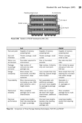
Stacked ICs and Packages (SIP)      119


                                   Flexible printed circuit       Au stud bump


                                                                            LSI chip A
                            Solder bumps


                                                                              LSI chip B


                    FIGURE 3.48  Variation of FSCSP developed by NEC. [52]


                              PoP                   PiP                   FSCSP
                Test and yield  Capable of memory   Capable of memory     Capable of memory
                              screening test        screening test        screening test
                Size and      Thicker package, small   Thicker package, small   Thicker package,
                thickness     xy size               xy size               small xy size
                Silicon bus   Four-sided required for   One- or four-sided   One side only (fold
                architecture  interconnect          possible              side)
                Package-      High number of        High number, limited by   150, limited by power
                to-package    connects but adds     only wire bond pitch  and ground ratio and
                connects      package size                                fold size
                Design        Most simple, two-     Less complex than chip   More simple than chip
                complexity    bond shells, nice BGA   stacking; special design   stacking but one-sided
                              interconnect, large   tools needed          fold makes design
                              substrate                                   complex
                Expandability  More interconnects by   Not expandable with   Stackable in z
                              increasing xy size, BGA   additional packages   direction with
                              pitch reduction, and z  but much more capable   2+ packages on
                              height stacks         for package-to-package   packages
                                                    connects
                Mechanical    More compliant        Stiffer due to silicon   More compliant
                reliability   package due to multi-  die stack with single   package due to multi-
                              interconnects         interconnect, additional   interconnects
                                                    thickness
                Electrical    Longer trace lengths   Shortest trace lengths   Long trace lengths
                performance   than chip stacking due   besides chip stacking,   around fold requiring
                              to larger xy package   long package-to-     shield
                              size                  package wire
               TABLE 3.1  Comparison of Three Package Stacking Technologies: PoP, PiP, and FSCSP