
Page 139 - System on Package_ Miniaturization of the Entire System
P. 139
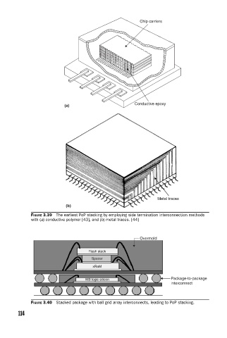
Chip carriers


                                                              Conductive epoxy
                                  (a)


                                                                        Metal traces
                                  (b)

                    FIGURE 3.39  The earliest PoP stacking by employing side termination interconnection methods
                    with (a) conductive polymer [43], and (b) metal traces. [44]


                                                                 Overmold

                                            Flash stack
                                             Spacer
                                             xRaM

                                          WB logic silicon                   Package-to-package
                                                                             interconnect


                    FIGURE 3.40  Stacked package with ball grid array interconnects, leading to PoP stacking.

               114