
Page 135 - System on Package_ Miniaturization of the Entire System
P. 135
110 Cha pte r T h ree
interconnection for edge mounting of a chip onto a bottom base chip [38]. In this
solder interconnection, solder bumps are formed along the edge of a vertically placed
chip to contact pads on the bottom base chip during solder reflow, yielding arch-
shaped solder column interconnections. This solder interconnection shows the
capability to stack chips on a single base chip. The arched solder columns offer several
electrical and mechanical advantages. The circular cross section is an excellent
geometry for electric signal propagation as it provides a controlled transition for
microwave and millimeter wave signals. The arched columns may also provide
structural support, while allowing some compliance for improved reliability, in
contrast to traditional rigid fillet shapes.
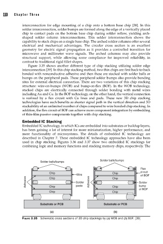
Figure 3.35 shows another different type of chip stacking utilizing solder edge
interconnection [39]. In this chip stacking method, two thin chips are first back-to-back
bonded with nonconductive adhesive and then these are stacked with solder balls or
bumps on the peripheral pads. These peripheral solder bumps also provide bonding
sites for external electrical connection. There are two variations of this chip stacking
structure: wire-on-bumps (WOB) and bump-on-flex (BOF). In the WOB technology,
stacked chips are electrically connected through solder bonding with metal wires
including Au and Cu. In the BOF technology, on the other hand, the vertical connection
is realized by a flex circuit with Cu lines and pads. These new 3D chip stacking
technologies have such benefits as shorter signal path in the vertical direction and 3D
stackability of an unlimited number of chips compared to wire bonded chip stacking. In
addition, the flex circuit of BOF can achieve more component integration by embedding
of thin-film passive components together with chip stacking.
Embedded IC Stacking
Embedded IC technology, in which ICs are embedded into substrates or buildup layers,
has been gaining a lot of interest for more miniaturization, higher performance, and
more functionality of microsystems. The details of embedded IC technology are
described in Chapter 7. These embedded IC technology approaches have also been
used in chip stacking. Figures 3.36 and 3.37 show two embedded IC stackings for
combining logic and memory functions and stacking memory chips, respectively. The
Solder balls/bumps Solder balls/bumps
Flex
circuit
Chip Chip
Wire of BOF
Adhesive Chip Solder Adhesive Chip Solder
Chip
paste
bump
Chip
Chip
of BOF
Chip Chip
Substrate or PCB Substrate or PCB
(a) (b)
FIGURE 3.35 Schematic cross sections of 3D chip stackings by (a) WOB and (b) BOF. [39]