
Page 133 - System on Package_ Miniaturization of the Entire System
P. 133
108 Cha pte r T h ree
Chip pads Wafer Passivation of Chip
rerouting thinning wafer backside singulation
Chip Sidewall Sidewall Opening of sidewall
stacking polishing passivation passivation layer
Metal trace Mounting of chip
deposition stack on substrate
FIGURE 3.31 Process fl ow for side-metallization chip stacking.
placed one on top of another to form a stack. In the side termination interconnection of
the stacked chips, polishing of the sidewall of stacked chips is needed. The passivation
layer is again deposited on all the polished sidewalls of the stacked chips, and openings
are made in the passivation layer above the desired electrical connection pads. Finally,
vertically adjacent chips are electrically interconnected by depositing metal traces on
the sidewall of the stack. This stack is then mounted on substrate.
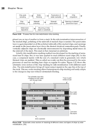
Initially, this metallization stacking method was developed for the stacking of same-
sized bare Si chips. But, it was later applied to stack different sized chips [36]. In this
case, a compound matrix with the size of a standard wafer is generated, into which
thinned chips are molded. This so-called neo-wafer can then be processed by the same
processes as used for stacking bare chips on regular Si wafers. Figure 3.32 shows the
schematic cross section of the chip stacking by side-metallization with different sized
dies. The side-metallization brings all input-output signals to the cap chip at the top of
the stack. This neo-wafer stacking allows heterogeneous chip stacking and easily adapts
to the change in chip size without substantial retooling.
Top substrate (cap chip),
metalized on both sides Trace to gold
with through holes wirebond pad
Bus metal
Chip
(two sides)
Chip Chip
Chip
Molding
Chip Chip
Laminated
chip layers
Blank substrate
FIGURE 3.32 Schematic cross section of stacking of different sizes and types of chips by side-
metallization. [36]