
Page 134 - System on Package_ Miniaturization of the Entire System
P. 134
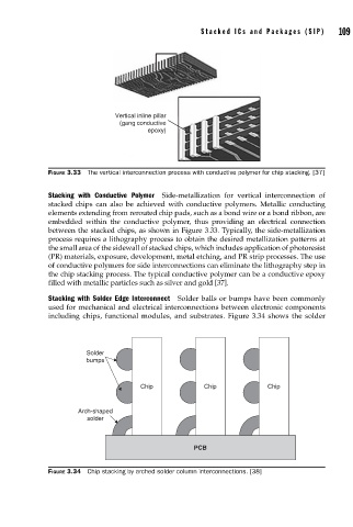
Stacked ICs and Packages (SIP)      109


                                      Vertical inline pillar
                                       (gang conductive
                                              epoxy)


                    FIGURE 3.33  The vertical interconnection process with conductive polymer for chip stacking. [37]


                    Stacking with Conductive Polymer  Side-metallization for vertical interconnection of
                    stacked chips can also be achieved with conductive polymers. Metallic conducting
                    elements extending from rerouted chip pads, such as a bond wire or a bond ribbon, are
                    embedded within the conductive polymer, thus providing an electrical connection
                    between the stacked chips, as shown in Figure 3.33. Typically, the side-metallization
                    process requires a lithography process to obtain the desired metallization patterns at
                    the small area of the sidewall of stacked chips, which includes application of photoresist
                    (PR) materials, exposure, development, metal etching, and PR strip processes. The use
                    of conductive polymers for side interconnections can eliminate the lithography step in
                    the chip stacking process. The typical conductive polymer can be a conductive epoxy
                    filled with metallic particles such as silver and gold [37].

                    Stacking with Solder Edge Interconnect  Solder balls or bumps have been commonly
                    used for mechanical and electrical interconnections between electronic components
                    including chips, functional modules, and substrates. Figure 3.34 shows the solder


                              Solder
                              bumps


                                            Chip             Chip             Chip


                            Arch-shaped
                              solder


                                                          PCB


                    FIGURE 3.34  Chip stacking by arched solder column interconnections. [38]