
Page 129 - System on Package_ Miniaturization of the Entire System
P. 129
104 Cha pte r T h ree
Electrical Routing Considerations In general, DRAM and flash memory have inter-
connections on only two sides of the die, splitting the address and data bus. In addition,
the memory chips can have different bond options, as 16 or 32 bit, and can even have one-
or two-sided bonding options. These various options change the order of signal sequencing
on the die and must be accounted for in the wire bonded chip-stack design. Stacking of
logic ICs with memory chips also brings electrical routing issues. It is very common to
have a logic die that has a flash bus on one side and a double data rate (DDR) bus on the
other, stacked with an external DDR and flash that are two-sided. These widely different
pad placements make the substrate routing and integration even more difficult.
In order to effectively stack chips, the pad ring sequencing of different die in the
stack should be such that it allows the bond wires to land on the bond fingers with
minimal overlap or cross. This ensures stackability, routability, the highest electrical
performance, and the lowest cost by simplifying the interconnect methodology. This
methodology could enable multiple wires to be bonded to the same bond pad. Since
only one bond finger is needed for two or more signals, the decrease in bond fingers
allows much more substrate routing flexibility.
Flip Chip Stacking
An alternative to the wire bonding interconnection in chip stacking is flip chip. Flip
chip has been used for more than three decades to increase the electrical performance
by decreasing the electrical length of the interconnection between the chip and the rest
of the system and by allowing a higher number of connections by utilizing the entire
area of the chip. The flip chip interconnection has been used for chip stacking, either on
its own or as a complement to wire bonding. The possible applications of this stacking
technology are for high-performance workstations, servers, data communication
products, internet routers, and other high-frequency and RF systems.
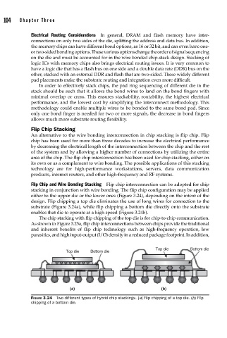
Flip Chip and Wire Bonding Stacking Flip chip interconnection can be adopted for chip
stacking in conjunction with wire bonding. The flip chip configuration may be applied
either to the upper die or the lower ones (Figure 3.24), depending on the intent of the
design. Flip chipping a top die eliminates the use of long wires for connection to the
substrate (Figure 3.24a), while flip chipping a bottom die directly onto the substrate
enables that die to operate at a high speed (Figure 3.24b).
The chip stacking with flip chipping of the top die is for chip-to-chip communication.
As shown in Figure 3.25a, flip chip interconnections between chips provide the traditional
and inherent benefits of flip chip technology such as high-frequency operation, low
parasitics, and high input-output (I/O) density in a reduced package footprint. In addition,
Top die Bottom die
Top die Bottom die
(a) (b)
FIGURE 3.24 Two different types of hybrid chip stackings. (a) Flip chipping of a top die. (b) Flip
chipping of a bottom die.