
Page 126 - System on Package_ Miniaturization of the Entire System
P. 126
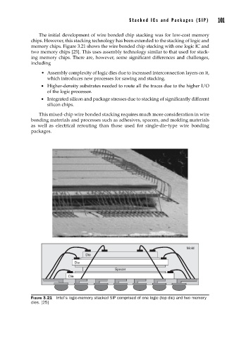
Stacked ICs and Packages (SIP)      101


                       The initial development of wire bonded chip stacking was for low-cost memory
                    chips. However, this stacking technology has been extended to the stacking of logic and
                    memory chips. Figure 3.21 shows the wire bonded chip stacking with one logic IC and
                    two memory chips [25]. This uses assembly technology similar to that used for stack-
                    ing memory chips. There are, however, some significant differences and challenges,
                    including
                        •  Assembly complexity of logic dies due to increased interconnection layers on it,
                           which introduces new processes for sawing and stacking.
                        •  Higher-density substrates needed to route all the traces due to the higher I/O
                           of the logic processor.
                        •  Integrated silicon and package stresses due to stacking of significantly different
                           silicon chips.
                       This mixed-chip wire bonded stacking requires much more consideration in wire
                    bonding materials and processes such as adhesives, spacers, and molding materials
                    as well as electrical rerouting than those used for single-die-type wire bonding
                    packages.


                                                                                    Mold
                                          Die
                                      Die
                                                      Spacer
                                   Die


                    FIGURE 3.21  Intel’s logic-memory stacked SIP comprised of one logic (top die) and two memory
                    dies. [25]