Page 122 - System on Package_ Miniaturization of the Entire System
P. 122

Stacked ICs and Packages (SIP)      97


                           900
                           800     Wafer thickness

                           700
                       Wafer diameter (mm)/ wafer and chip thickness (μm)  600  Chip thickness DIP  PDIP  TQFP  Wafer diameter

                           500
                           400
                                                               BGA
                                                                TSSOP
                           300
                           300
                                                                          Stack
                           200
                           100                                  CSP     modules
                            0
                             1960     1970      1980      1990      2000      2010      2020
                                                  Year of significant production
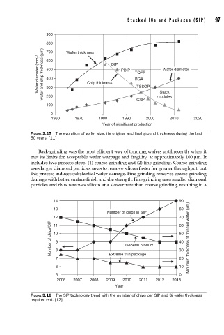
                    FIGURE 3.17  The evolution of wafer size, its original and fi nal ground thickness during the last
                    50 years. [11]

                       Back-grinding was the most efficient way of thinning wafers until recently when it
                    met its limits for acceptable wafer warpage and fragility, at approximately 100 μm. It
                    includes two process steps: (1) coarse grinding and (2) fine grinding. Coarse grinding
                    uses larger diamond particles so as to remove silicon faster for greater throughput, but
                    this process induces substantial wafer damage. Fine grinding removes coarse grinding
                    damage with better surface finish and die strength. Fine grinding uses smaller diamond
                    particles and thus removes silicon at a slower rate than coarse grinding, resulting in a


                              14                                                  90
                              13                                                  80
                                                    Number of chips in SIP
                              12                                                  70
                            Number of chips/SIP  10 9      General product        50  Minimum thickness of thinned wafer (μm)
                              11
                                                                                  60

                                                                                  40


                               7 8                   Extreme thin package         30
                                                                                  20
                               6                                                  10

                               5                                                  0
                               2006   2007   2008  2009   2010   2011   2012   2013
                                                       Year
                    FIGURE 3.18  The SIP technology trend with the number of chips per SIP and Si wafer thickness
                    requirement. [12]
   117   118   119   120   121   122   123   124   125   126   127