
Page 127 - System on Package_ Miniaturization of the Entire System
P. 127
102 Cha pte r T h ree
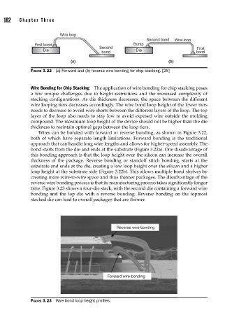
Wire loop
Second bond Wire loop
First bond Bump
Second First
Die Die
bond bond
(a) (b)
FIGURE 3.22 (a) Forward and (b) reverse wire bonding for chip stacking. [26]
Wire Bonding for Chip Stacking The application of wire bonding for chip stacking poses
a few unique challenges due to height restrictions and the increased complexity of
stacking configurations. As die thickness decreases, the space between the different
wire looping tiers decreases accordingly. The wire bond loop height of the lower tiers
needs to decrease to avoid wire shorts between the different layers of the loop. The top
layer of the loop also needs to stay low to avoid exposed wire outside the molding
compound. The maximum loop height of the device should not be higher than the die
thickness to maintain optimal gaps between the loop tiers.
Wires can be bonded with forward or reverse bonding, as shown in Figure 3.22,
both of which have separate length limitations. Forward bonding is the traditional
approach that can handle long wire lengths and allows for higher-speed assembly. The
bond starts from the die and ends at the substrate (Figure 3.22a). One disadvantage of
this bonding approach is that the loop height over the silicon can increase the overall
thickness of the package. Reverse bonding or standoff stitch bonding, starts at the
substrate and ends at the die, creating a low loop height over the silicon and a higher
loop height at the substrate side (Figure 3.22b). This allows multiple bond shelves by
creating more wire-to-wire space and thus thinner packages. The disadvantage of the
reverse wire bonding process is that its manufacturing process takes significantly longer
time. Figure 3.23 shows a four-die stack, with the second die containing a forward wire
bonding and the top die with a reverse bonding. Reverse bonding on the topmost
stacked die can lead to overall packages that are thinner.
Reverse wire-bonding
Forward wire-bonding
FIGURE 3.23 Wire bond loop height profi les.