
Page 132 - System on Package_ Miniaturization of the Entire System
P. 132
Stacked ICs and Packages (SIP) 107
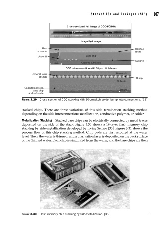
Cross-sectional full image of COC-FCBGA
Magnified image
Heat Silicone
spreader resin
Underfill Base chip
Subchip
1 mm Organic substrate
COC interconnection with 30 μm pitch bump
Underfill resin Base chip
at COC
Bump
Subchip
Underfill between
base chip 50 um
and substrate
FIGURE 3.29 Cross section of COC stacking with 30-μm-pitch solder bump interconnections. [33]
stacked chips. There are three variations of this side termination stacking method
depending on the side interconnection: metallization, conductive polymer, or solder.
Metallization Stacking Stacked bare chips can be electrically connected by metal traces
deposited on the side of the stack. Figure 3.30 shows a 19-layer flash memory chip
stacking by side-metallization developed by Irvine Sensor [35]. Figure 3.31 shows the
process flow of this chip stacking method. Chip pads are first rerouted at the wafer
level. Then, the wafer is thinned, and a passivation layer is deposited on the back surface
of the thinned wafer. Each chip is singulated from the wafer, and the bare chips are then
FIGURE 3.30 Flash memory chip stacking by side-metallization. [35]