
Page 150 - System on Package_ Miniaturization of the Entire System
P. 150
Stacked ICs and Packages (SIP) 125
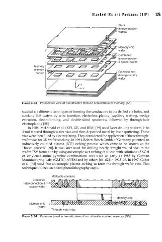
Stack
interconnection
wafers
Memory chip
wafer
Combined
interconnection
& spacer wafer
Memory
element
portion Selection and
driving circuitry
wafer
z
y
x
FIGURE 3.53 Perspective view of a multiwafer stacked semiconductor memory. [55]
studied six different techniques of forming the conductors in the drilled via holes, and
stacking SoS wafers by wire insertion, electroless plating, capillary wetting, wedge
extrusion, electroforming, and double-sided sputtering followed by through-hole
electroplating [58].
In 1986, McDonald et al. (RPI, GE, and IBM) [59] used laser drilling to form 1- to
3-mil tapered through-wafer vias and then deposited metal by laser sputtering. These
vias were then filled by electroplating. They considered the application of these through-
wafer vias for 3D wafer stacking. In 1994, Robert Bosch Gmbh of Germany patented an
inductively coupled plasma (ICP) etching process which came to be known as the
“Bosch process” [60]. It was later used for drilling nearly straight-walled vias in the
wafer. TSV formation by using anisotropic wet etching of silicon with solutions of KOH
or ethylenediamine-pyrazine combinations was used as early as 1985 by German
Manufacturing Labs (GMTC) of IBM and by others [61–62] in 1995–96. In 1997, Gobet
et al. [63] used fast anisotropic plasma etching to form the through-wafer vias. This
technique utilized standard photolithography steps.
Malleable contacts
Combined
interconnection &
spacer wafer
Memory chip
Memory chip
wafer
Through-wafer vias
FIGURE 3.54 Cross-sectional schematic view of a multiwafer stacked memory. [55]