Page 161 - System on Package_ Miniaturization of the Entire System
P. 161

Top metal layers
                                                 IMD gapfill and oxide CMP
                                                                             Device and
                               Device and IMD layers  Device and IMD layers
                                                                             IMD layers
                                   Si base            Si base             Si base
                                   Step 1             Step 2               Step 3

                                                       SiO 2 /SiN


                                     Device and          Device and          Device and
                                     IMD layers          IMD layers           IMD layers
                                      Si base             Si base             Si base

                                   Step 4              Step 5              Step 6
                                                    Cu metal            Cu metal
                                      Device and         Device and         Device and
                                      IMD layers         IMD layers         IMD layers
                                       Si base            Si base            Si base

                                    Step 7            Step 8              Step 9

                                                           Si Base


                                                     Cu metal           Cu metal
                                  Cu metal
                                      Device and         Device and         Device and
                                      IMD layers         IMD layers         IMD layers
                                       Si base            Si base            Si base

                                   Step 10            Step 11            Step 12

                                   Backside ILD                          Cu metal

                                                         2 nd  wafer         2 nd  wafer


                                Cu metal             Cu metal            Cu metal


                                     Device and          Device and          Device and
                                      IMD layers         IMD layers          IMD layers
                                      Si base
                                                          1 st  wafer        1 st  wafer

                                  Step 13             Step 14             Step 15
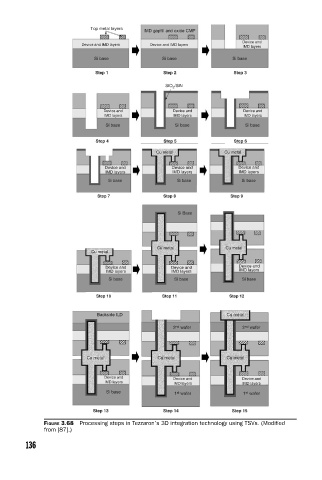
                    FIGURE 3.68  Processing steps in Tezzaron’s 3D integration technology using TSVs. (Modifi ed
                    from [87].)

               136
   156   157   158   159   160   161   162   163   164   165   166