
Page 166 - System on Package_ Miniaturization of the Entire System
P. 166
Stacked ICs and Packages (SIP) 141
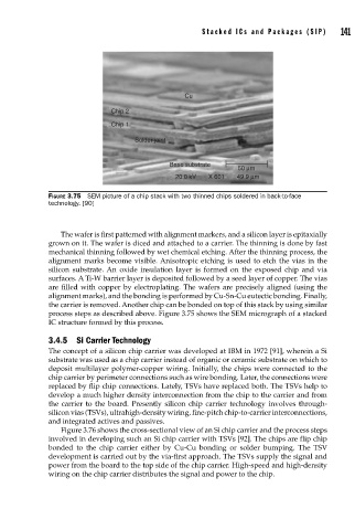
Cu
Chip 2
Chip 1
Solder joint
Base substrate
50 μm
20.0 kV X 601 49.9 μm
FIGURE 3.75 SEM picture of a chip stack with two thinned chips soldered in back-to-face
technology. [90]
The wafer is first patterned with alignment markers, and a silicon layer is epitaxially
grown on it. The wafer is diced and attached to a carrier. The thinning is done by fast
mechanical thinning followed by wet chemical etching. After the thinning process, the
alignment marks become visible. Anisotropic etching is used to etch the vias in the
silicon substrate. An oxide insulation layer is formed on the exposed chip and via
surfaces. A Ti-W barrier layer is deposited followed by a seed layer of copper. The vias
are filled with copper by electroplating. The wafers are precisely aligned (using the
alignment marks), and the bonding is performed by Cu-Sn-Cu eutectic bonding. Finally,
the carrier is removed. Another chip can be bonded on top of this stack by using similar
process steps as described above. Figure 3.75 shows the SEM micrograph of a stacked
IC structure formed by this process.
3.4.5 Si Carrier Technology
The concept of a silicon chip carrier was developed at IBM in 1972 [91], wherein a Si
substrate was used as a chip carrier instead of organic or ceramic substrate on which to
deposit multilayer polymer-copper wiring. Initially, the chips were connected to the
chip carrier by perimeter connections such as wire bonding. Later, the connections were
replaced by flip chip connections. Lately, TSVs have replaced both. The TSVs help to
develop a much higher density interconnection from the chip to the carrier and from
the carrier to the board. Presently silicon chip carrier technology involves through-
silicon vias (TSVs), ultrahigh-density wiring, fine-pitch chip-to-carrier interconnections,
and integrated actives and passives.
Figure 3.76 shows the cross-sectional view of an Si chip carrier and the process steps
involved in developing such an Si chip carrier with TSVs [92]. The chips are flip chip
bonded to the chip carrier either by Cu-Cu bonding or solder bumping. The TSV
development is carried out by the via-first approach. The TSVs supply the signal and
power from the board to the top side of the chip carrier. High-speed and high-density
wiring on the chip carrier distributes the signal and power to the chip.