
Page 165 - System on Package_ Miniaturization of the Entire System
P. 165
140 Cha pte r T h ree
Si IC 2
20 μm
Si IC 1
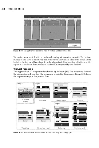
FIGURE 3.73 An SEM cross-sectional view of vertically stacked ICs. [89]
Via surfaces are coated with a conformal coating of insulator material. The bottom
surface of this layer is selectively removed before the vias are filled with metal. In the
last step, the top metal layer is patterned and passivated for bonding with the next die.
Figure 3.73 shows an SEM picture of stacked ICs integrated by this method.
Via-Last Process 3
This approach of 3D integration is followed by Infineon [90]. The wafers are thinned,
the vias are formed, and then the wafers are bonded in this process. Figure 3.74 shows
the important steps in this process flow.
Stage 1 Stage 2
Carrier
Cu Cu
Wiring
CMOS
Si Si
Si Si epitaxy Carrier
+
p epitaxy
Front metal Glue to carrier Thinning
Epitaxy
Stage 3
Carrier
Sn
Cu Cu
Carrier Carrier
Cu Cu Cu Cu
Si Si
Via etching Via and rear metal Soldering Carrier removal
FIGURE 3.74 Process fl ow for Infi neon’s 3D chip stacking technology. [90]