
Page 115 - System on Package_ Miniaturization of the Entire System
P. 115
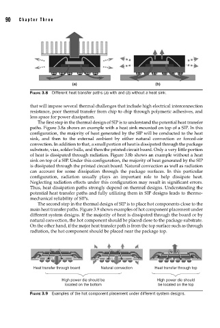
90    Cha pte r  T h ree


                                      (a)                                (b)
                    FIGURE 3.8  Different heat transfer paths (a) with and (b) without a heat sink.


                    that will impose several thermal challenges that include high electrical interconnection
                    resistance, poor thermal transfer from chip to chip through polymeric adhesives, and
                    less space for power dissipation.
                       The first step in the thermal design of SIP is to understand the potential heat transfer
                    paths. Figure 3.8a shows an example with a heat sink mounted on top of a SIP. In this
                    configuration, the majority of heat generated by the SIP will be conducted to the heat
                    sink, and then to the external ambient by either natural convection or forced-air
                    convection. In addition to that, a small portion of heat is dissipated through the package
                    substrate, vias, solder balls, and then the printed circuit board. Only a very little portion
                    of heat is dissipated through radiation. Figure 3.8b shows an example without a heat
                    sink on top of a SIP. Under this configuration, the majority of heat generated by the SIP
                    is dissipated through the printed circuit board. Natural convection as well as radiation
                    can account for some dissipation through the package surfaces. In this particular
                    configuration, radiation usually plays an important role to help dissipate heat.
                    Neglecting radiation effects under this configuration may result in significant errors.
                    Thus, heat dissipation paths strongly depend on thermal designs. Understanding the
                    potential heat transfer paths and fully utilizing them in SIP designs leads to thermo-
                    mechanical reliability of SIPs.
                       The second step in the thermal design of SIP is to place hot components close to the
                    main heat transfer paths. Figure 3.9 shows examples of hot component placement under
                    different system designs. If the majority of heat is dissipated through the board or by
                    natural convection, the hot component should be placed close to the package substrate.
                    On the other hand, if the major heat transfer path is from the top surface such as through
                    radiation, the hot component should be placed near the package top.


                      Heat transfer through board  Natural convection    Heat transfer through top


                                  High power die should be                High power die should
                                   located on the bottom                  be located on the top
                    FIGURE 3.9  Examples of the hot component placement under different system designs.