
Page 108 - System on Package_ Miniaturization of the Entire System
P. 108
I/O per cm 2
Challenge
Potential disruptive
technology
Advantages
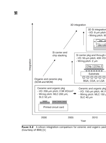
3D Si integration and pkg 3D chip integration Cooling 3D wiring Yield Net length - I/O: 6-mm pitch; 2.5M I/O/cm 2 —10 5 to 10 8 Design Performance - Wiring pitch: 90 nm Test Alignment Assembly Si carrier pkg and through-via stacking - I/O: 50-μm pitch; 40K I/O/cm 2 Chip stack and Test Modular design chip to Si carrier Assembly Performa
3D integration - Wiring pitch: 2 mm Chip 1 SLC 40 mm 2005 Year
Si carrier and chip stacking - I/O: 200-mm pitch; 2.5K I/O/cm 2
Organic and ceramic pkg (SCM and MCM) Ceramic and organic pkg - Wiring pitch: MLC 200 mm; SLC 50 mm Printed circuit card 2000
FIGURE 3.2 (Courtesy of IBM) [1]
Integration
84