
Page 248 - MEMS Mechanical Sensors
P. 248
9.4 Force Transfer Flow Sensors 237
Flow out
Flow in F C
θ C
θ exc
F C
Excitation electrode
Figure 9.29 Coriolis force loop twisting due to mass flow. (After: [96].)
high-linearity position photodetector. The amplitude of the induced angular motion
is linearly proportional to the mass flow and therefore a measure of the flow. A
single-loop configuration is possible for Coriolis mass-flow sensing, but the bal-
anced double-loop configuration gives a higher Q value and relatively large ampli-
tudes and hence easier detection [96].
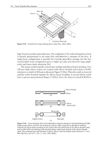
The sensor is fabricated by anisotropic etching and silicon fusion bonding. Two
500-µm-thick silicon wafers are masked with silicon dioxide and etched in KOH-
solution to a depth of 400 µm as shown in Figure 9.30(a). Then the oxide is removed
and the wafers bonded together by silicon fusion bonding. A second silicon oxide
layer is grown and patterned [Figure 9.30(b)]. Next, the wafer is etched in KOH to
Silicon dioxide
Silicon
(a)
Silicon
fusion bond
(b)
Silicon tube
Support frame Fluid path
(c)
Figure 9.30 Cross-sectional view of the fabrication sequence based on micromachining of (100)
single-crystal silicon: (a) KOH wet etching of a silicon wafer using silicon dioxide as masking
material; (b) silicon fusion bonding of two wafers after the patterning of the silicon dioxide mask;
and (c) after KOH wet etching of the bonded silicon wafers and removal of the silicon dioxide
mask. The resulting tube wall thickness is about 100 µm and the double wafer thickness is 1 mm.
3
The chip has a size of 9 × 18 × 1mm .(After: [96].)