
Page 52 - MEMS and Microstructures in Aerospace Applications
P. 52
Osiander / MEMS and microstructures in Aerospace applications DK3181_c003 Final Proof page 42 1.9.2005 8:59pm
42 MEMS and Microstructures in Aerospace Applications
NH 4 F $ NH 3 þ HF (3:2)
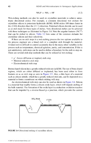
Wet-etching methods can also be used on crystalline materials to achieve aniso-
tropic directional etches. For example, a common directional wet etchant for
crystalline silicon is potassium hydroxide (KOH). KOH etches 100 times faster in
the (1 0 0) direction than the (1 1 1) direction. Patterned silicon dioxide can be used
as an etch mask for these types of etches. Very directional etches can be achieved
with these techniques as illustrated in Figure 3.4. Note the angular features (54.7 8)
that can be etched in silicon. Table 3.2 lists some of the common etchants for
crystalline silicon and their selectivity.
If there are no etch stops in a wet-etching process the two options available to
the process engineer are a timed etch or a complete etch through the material.
A timed etch is difficult to control accurately due to the many other variables in the
process such as temperature, chemical agitation, purity, and concentration. If this is
not satisfactory, etch stops can be used to define a boundary for the etch to stop on.
There are several etch-stop methods that can be utilized in wet etching:
þ
. p (boron diffusion or implant) etch stop
. Material-selective etch stop
. Electrochemical etch stop
Boron-doped silicon has a greatly reduced etch rate in KOH. The use of born-doped
regions, which are either diffused or implanted, has been used either to form
features or as an etch stop as seen in Figure 3.5. Also, a thin layer of a material
such as silicon nitride, which has a greatly reduced etch rate, can be deposited on a
material to form a membrane on which etching will stop.
An electrochemical etch stop can also be used as shown in Figure 3.6. Silicon
is a material that readily forms a silicon oxide layer, which will impede etching of
the bulk material. The formation of the oxide layer is a reduction–oxidation reaction
that can be impeded by a reverse-biased p–n junction, which prevents the current h
SiO 2 Mask
<100>
φ = 54.7
φ
<111>
FIGURE 3.4 Directional etching of crystalline silicon.
© 2006 by Taylor & Francis Group, LLC