
Page 56 - MEMS and Microstructures in Aerospace Applications
P. 56
Osiander / MEMS and microstructures in Aerospace applications DK3181_c003 Final Proof page 46 1.9.2005 8:59pm
46 MEMS and Microstructures in Aerospace Applications
called polymerization and is controlled by the ratio of fluoride to carbon in the
reactants. The sidewall deposits produced by polymerization can only be removed
by physical ion collisions. Etch products from the resist masking are also involved
in the polymerization.
Etch endpoint detection is important in controlling the etch depth or minimizing
the damage to underlying films. Endpoint detection is accomplished by analysis of
the etch effluents or spectral analysis of the plasma glow discharge to detect.
The type of plasma etches include reactive ion etching (RIE), high-density
plasma etching (HDP), and deep reactive ion etching (DRIE). RIE utilizes low-
pressure plasma. Chlorine (Cl)-based plasmas are commonly used to etch silicon,
GaAs, and Al. RIE may damage the material due to the impacts of the ions. The
damage can be mitigated by annealing at high temperatures. HDP etches utilize
magnetic and electric fields to dramatically increase the distance that free electrons
can travel in the plasma. HDP etches have good selectivity of Si to SiO 2 and
resist. The DRIE etch cycles between the etch chemistry and deposition of the
sidewall polymer, which enables the high aspect ratio and vertical sidewalls attain-
able with this process. 16
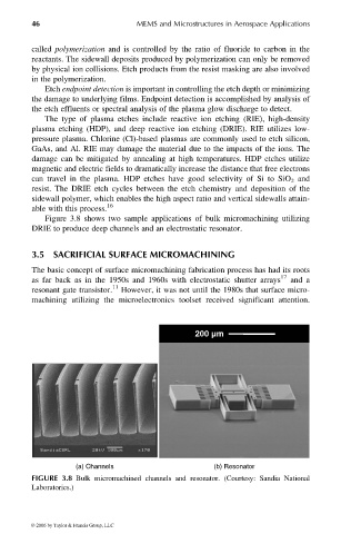
Figure 3.8 shows two sample applications of bulk micromachining utilizing
DRIE to produce deep channels and an electrostatic resonator.
3.5 SACRIFICIAL SURFACE MICROMACHINING
The basic concept of surface micromachining fabrication process has had its roots
as far back as in the 1950s and 1960s with electrostatic shutter arrays 17 and a
resonant gate transistor. 11 However, it was not until the 1980s that surface micro-
machining utilizing the microelectronics toolset received significant attention.
200 µm
(a) Channels (b) Resonator
FIGURE 3.8 Bulk micromachined channels and resonator. (Courtesy: Sandia National
Laboratories.)
© 2006 by Taylor & Francis Group, LLC