
Page 60 - MEMS and Microstructures in Aerospace Applications
P. 60
Osiander / MEMS and microstructures in Aerospace applications DK3181_c003 Final Proof page 50 1.9.2005 8:59pm
50 MEMS and Microstructures in Aerospace Applications
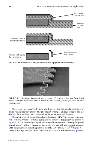
Conformable
structural layer
Patterned
sacrificial
layer
Anisotropic etch of
top structural layer
Floating structural
Release etch leaving layer “stringer”
floating stringer
FIGURE 3.11 Illustration of stringer formation at a topographical discontinuity.
FIGURE 3.12 Scanning electron microscope image of a stringer that was formed and
floated to another location on the die during the release etch. (Courtesy: Sandia National
Laboratories.)
The second process difficulty is the challenge of photolithographic definition of
layers with severe topography. The photoresist coating is difficult to apply and the
depth of focus will lead to a decreased resolution of patterned features.
The application of chemical mechanical polishing (CMP) to surface microma-
chine MEMS processes directly addresses the issues of topography as shown in
Figure 3.13. CMP was originally utilized in the microelectronics industry for global
21
planarization, which is needed as the levels of electrical interconnect increase.
22,23
CMP planarization was first reported in the MEMS by Nasby et al. Figure 3.14
shows a linkage that has been fabricated in a surface micromachined process,
© 2006 by Taylor & Francis Group, LLC